• home

Solid State Relays Circuit with TIL111

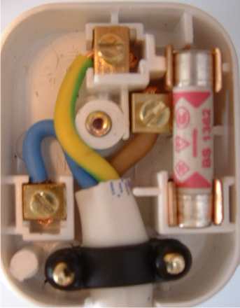
Solid state relays are almost everywhere these days, but they are very expensive. So, your efforts to build their own salary. Especially since it’s only a few parts and circuit simple and straightforward. Solid state relay is not really at all relays. There are no “relay” is available only with electronics, connection works. It works well as a relay, you can use low voltage higher and better. “Relay” between 115/220V AC wires in place, although it was customary, the neutral conductor and leave unchanged phases and neutral.

As long as no voltage (left in picture), the phototransistor TIL111 blocks of energy, and thus is not available. To ensure that the base TIL111 is fed to the transmitter (s) through the 1M resistor. This method prevents the base of transistor BC547B will be low and remains biased ‘on’. Collector is low and the gate (g) TIC106M thyristor, which is still in the country, “off”. 4-diode bridge rectifier circuit has no power apart from a small base and collector current BC547B, which is not enough to turn over the 330-ohm resistor TIC226M triac. Current “Load”, is very small.

Solid State Relays Circuit Diagram

With an input voltage, say 5 volts, the diode in the TIL111 lights up and activates the phototransistor. The voltage drop 1MEG ohm resistor in series with 22K resistance increases demand, which block the BC547B transistor. Collector current of the fact that the AC voltage falls below a certain value, which is VA. This ensures a sufficiently large voltage drop across the resistor 330 ohms triac switches ‘on’. The voltage on triac is currently only a few volts, so that practically the whole 115/220 AC voltage on the “Upload”.

The triac is a 100nF capacitor and impedance of 47 ohms, 100nF capacitor for the 330 ohm resistor is to protect the triac to be undesirable distortions caused by small peaks. To create the possibility of this circuit with different voltages to be switched, added BF256A FET. The FET acts as a current source from the source (s) with a gate (g). This means that this FET determines the current TIL111, regardless of the input voltage (up to a certain tolerance, of course). 1N4148 diode is to protect the circuit from reverse polarity.
(Tony: TIL111 is a so-called “optical coupling” with NPN output and can be replaced with NTE3042)

Good point line, as is the separation of AC and DC voltage, so this circuit is used in many applications, about 1.5 kW, when the triac is mounted on the large size of the cooling fins. “M” appears Triac means it’s 600volt type, “D” for 400V. So be sure to go to the M-type. NTE replacement for this circuit are 600volt types which are more than sufficient for our 110/115VAC. Even if you decide to print for this circuit is enough space between the lines AC and non AC these tracks to be close.

Basic Monostable Using with LM555

Welcome to free circuit dot com,For the last article in this series, we may be unstable a cycle which has no stable output state. In this post circuit we will show the monostable circuit, which has a stable state.

Basic Monostable Circuit diagram 


The waveforms in Figure 1 show the effect of a monostable. A monostable circuit produces a pulse of a certain length (time T) in response to a trigger input such as a pushbutton. The output of the circuit remains in the low position to a trigger input, does the name “Mono”, “stable condition”. This type of circuit is ideal for use in a “push-to-operate” in a model system for exhibitions.

A visitor can press a button to a model mechanism in motion, and the mechanism will automatically after a certain time. Another use of the circuit “the bounce” an important contribution to a digital IC – this application will be explained later in this article.

How to Make a Simplest Triac Dimmer Switch Circuit

We have already seen in many of my earlier articles how triacs are used in electronic circuits for switching AC loads.
Triacs are basically devices which are able to switch ON a particular connected load in response to an external DC trigger.
Though these may be incorporated for complete switch ON and complete switch OFF procedures of a load, the device is also popularly applied for regulating an AC, such that the output to the load may be reduced to any desired value.
For example triacs are very commonly used dimmer switch applications where the circuit is designed to make the device switch in such a manner that it conducts only for a particular section of the AC sine wave and remains cut OFF during the remaining parts of the sine wave.
This result is an corresponding output AC which has an average RMS value much lower than the actual input AC.
The connected load also responds to this lower value AC and is thus controlled to that particular consumption or resultant output.
This is what exactly happens inside electrical dimmer switches which are normally used for controlling ceiling fan and incandescent lights.

Simple and the Best Triac Dimmer Switch Circuit

The circuit diagram shown above is an classic example of a dimmer switch, where a triac has been utilized for controlling the intensity of light.
When AC mains is fed to the above circuit, as per the setting of the pot, C2 charges fully after a particular delay providing the necessary firing voltage to the diac.
The diac conducts and triggers the triac into conduction, however this also discharges the capacitor whose charge reduces below the diacs firing voltage.
Due to this the diac stops conducting and so does the triac.
This happens for each cycle of the mains AC sine wave signal, which cuts it into discrete sections, resulting in well tailored lower voltage output.
The setting of the pot sets the charge and the discharge timing of C2 which in turn decides for how long the triac remains in a conducting mode for the AC sine signals.
You might be interested to know why C1 is placed in the circuit, because the circuit would work even without it.
Its true, C1 is actually not required if the connected load is a resistive load like an incandescent lamp etc.
However if the load is an inductive type, the inclusion of C1 becomes very crucial.
Inductive loads have a bad habit of returning a part of the stored energy in the winding, back into the supply rails.
This situation can choke up C2 which then becomes unable to charge properly for initiating the next subsequent triggering.
C1 in this situation helps C2 to maintain is cycle by providing bursts of small voltages even after C2 has completely discharged, and thus maintains the correct switching rate of the triac.
Triac dimmer circuits have the property of generating a lot of RF disturbances in the air while operating and therefore an RC network becomes imperative with these dimmer switches for reducing the RF generations. The above circuit is shown without the feature and therefore will generate a lot of RF which might disturb sophisticated electronic audio systems.
The circuit of a dimmer switch illustrated below incorporate the necessary precautions for subsiding the above issue.


Build 20W MOSFET Power Amplifier Circuit with IFR9520 IFR520

As we are like to show you about audio and sound circuit ,I found the circuit which is good one for power amplifier with one MOSFET.

The output power of an operational amplifier is often increased by a complementary emiter follower.


20W power amp MOSFET

It can also be done with a MOSFET,but it is not a good idea to connect such a device as a complementary souce follower because the maximum output voltage of the opamp is then reduced appreciably by the gate-source control voltage of the MOSFET ,which can be a couple of volts.

Another approach is to connect two MOSFETs as a complementary drain follower.The (alternating) output current provided by the MOSFETs is limited by the level of the supply voltages and the saturateion voltages of T3 and T4 Resistor R8,together with R9,provides feedback for both the opamp and MOSFETs .

The open-loop amplification of the opampis,therefore,increased by (1+R8/R9).the closed-loop amplification of the complete amplifier is (1+R3/R2).

The current source formed by T1 and T2 is required for arreanging the quiescent current of T3 and T4 at 50 mA.The values of resistors R4 and R5 are such that,without the current source the voltage drop across the resistor resulting from the direct current through the opamp is not sufficient to switch on T3 and T4 .with the current source,and depending on the setting of P1,the voltages across R4 and R5 rise,which increases the quiescent current through T3 and T4.

In view of the temperature dependence of the quiescent current,T2 must be mounted on the common heat sink(c. 5 K/W) of the MOSFETs.

The output power is not less than 20 W into 8 ohm,at which level the harmonic distortion amounts to 0.075 per cent at 100 Hz to 0,135 per cent at 10 kHz.

9 Volt 2 Amp PSU Circuit

A simple 9 Volt 2 amp supply using a single IC regulator.

The circuit will work without the extra components, but for reverse polarity protection a 1N5400 diode is provided at the input, extra smoothing being provided by C1. The output stage includes C2 for extra filtering, if powering a logic circuit than a 100nF capacitor is also desirable to remove any high frequency switching noise.

Circuit diagram:

9 Volt 2 Amp PSU Circuit 9 Volt 2 Amp PSU Circuit Diagram

Notes:

There is little to be said about this circuit. All the work is done by the regulator. The 78S09 can deliver up to 2 amps continuous output whilst maintaining a low noise and very well regulated supply.

Author : Andy Collinson Copyright : zen22142

Zero Crossing Detector Circuit

Zero Crossing Detector circuit is basically an application of a comparator. In the article series Zero Crossing Detector with Op Amp is built using a comparator of an Op Amp IC741/351. The process of detection of this comparator is  0Volt input signal crossing point by making reference value at comparator 0Volt.


 The output of the Zero Crossing Detector circuit with Op Amp is wave-shaped box that detection result of the crossroads of 0 volt input signal.

A178 00206wiringplug Socket House Wallconstruction

Wiringplug on How To Wire A Plug  Plug Wiring
How To Wire A Plug Plug Wiring.


Wiringplug on Gcse Science Safety In Mains Circuits   Wikibooks  Open Books For An
Gcse Science Safety In Mains Circuits Wikibooks Open Books For An.


Wiringplug on Diy Telephone Extension Kit  Philex  Wiring Diagram Wrong
Diy Telephone Extension Kit Philex Wiring Diagram Wrong.


Wiringplug on Spark Plug Test Cable Harness And Wiring Diagram   Circuit Schematic
Spark Plug Test Cable Harness And Wiring Diagram Circuit Schematic.


Wiringplug on 1988 Honda Accord Spark Plug Wiring Diagram   Fixya
1988 Honda Accord Spark Plug Wiring Diagram Fixya.


Wiringplug on Schematic Illustrates The Mazda Bt 50 Glow Plug Relay Wiring Diagram
Schematic Illustrates The Mazda Bt 50 Glow Plug Relay Wiring Diagram.


Wiringplug on Here Is The Wiring Diagram Each Hot Wire Will Go Directly To One Of
Here Is The Wiring Diagram Each Hot Wire Will Go Directly To One Of.


Wiringplug on How To Wire A Plug
How To Wire A Plug.


Wiringplug on Wiring A Switched Outlet Wiring Diagram   Electrical Online
Wiring A Switched Outlet Wiring Diagram Electrical Online.


Wiringplug on A178 00206  Wiring A Plug Socket Into A House Wall Uk   Construction
A178 00206 Wiring A Plug Socket Into A House Wall Uk Construction.


Green USB switch

According to the Energy Saving  Trust, if you add up all the current drawn in standby mode by items such as stereos, TVs, VCRs and DVDs over a year in the UK alone, it amounts to 3.1 million tonnes of CO2 released into the atmosphere.This is without factoring in the current drawn by all the PCs,laptops and their associated peripherals left in standby mode. 

Circuit diagram :
Green USB switch-Circuit Diagram
Green USB switch Circuit Diagram

It  is  not  necessary  to  spend  a  great deal of money or time to  make a difference on a personal  level. The circuit described here  is designed for use by laptop or  notebook computers. It will automatically switch off all mains  powered peripheral equipment  including monitor, printer, scanner, TV tuner and USB hub etc  when it detects that the notebook  is switched off. The circuit is quite  straightforward; in addition to an  optocoupler it requires a 12 V  double-pole  relay  with  mains  rated contacts and a small power  supply  for  the  optocoupler.  When the laptop is switched on  5 V appears at the USB socket,  activating the relay and switching  through  the  mains  supply  on K3 and K4. The notebook’s  USB socket is still available to be  used as normal but it’s worth remembering that the optocoupler  takes a few milliamps from the  USB supply and this may cause a  problem if a high-current device  is plugged into the USB socket.  In the case where the laptop has  more than enough USB sockets it may be worthwhile us-ing one of them solely for this  circuit, the extension USB connector K2 would then not be  required. 

The circuit is mounted into a  mains plug enclosure which  provides a socket where the  mains extension strip will be  plugged into. With any luck  there will be sufficient space  to fit the entire circuit into the  mains extension strip enclosure and save the need for a  separate enclosure. The slow-blow 6.3-A fuse (F1) protects  the equipment plugged into  the strip. 

In  addition  to  the  optocoupler  and relay the circuit also has a  ‘freewheel’ diode D1 and a relay  driver formed by T1 and its base  bias voltage divider network R2/ R4. The two ‘snubber’ networks  C1/R3 and C2/R5 reduce the  possibility of arcing which can  occur  when  the  relay  contacts  open (especially with inductive  loads). Capacitors C1 and C2  must be class X2 types which  can handle mains voltage plus any  spikes.  The  power  supply  consists of a small mains trans-former  (12 V,  50 mA),  bridge  rectifier and smoothing capacitor C3. 

The laptop’s mains adaptor itself  can also be switched by this circuit when the laptop is fitted with  its rechargeable battery which  allows the computer to boot up  without a mains supply. The en-tire USB switch circuit draws cur-rent even when it is off but this value  is  tiny  compared  to  the  combined standby current of all  the peripherals. 

Note that parts of this circuit are  connected to the (potentially lethal) mains supply voltage; it is  essential to provide protection  to ensure that nothing can accidentally make contact with these  parts of the circuit. It is also important to observe correct separation between parts of the circuit carrying low voltage and  those carrying the high volt-age. Please observe the electrical Electrical Safety guide-lines which are reprinted in  Elektor  Electronics  several  times a year. 

The  circuit  is  less  suitable  for use with desktop PCs be-cause  the  majority  of  these  machines supply 5 V over the  USB socket even though they  have been shut down via soft-ware. The only way to turn off  in this case is to reach around  the back of the machine and  switch off at the main switch. 


http://streampowers.blogspot.com/2012/06/green-usb-switch.html

Voltage Tester for Model Batteries

With a suitable load, the terminal voltage of a NiCd or lithium-ion battery is proportional to the quantity of saved power. This relationship, which is linear over a large range, will also be utilized to build a easy battery capability meter. 

Circuit Image :
 \"Voltage
Voltage Tester for Model Batteries Circuit Image 

This model battery tester has two carry outs: it gives a load for the battery, and on the similar time it measures the terminal voltage. In addition, each operates will moreover be switched on or off by the use of a adaptation remote-control receiver, to steer clear of draining the battery when it isn\'t essential to make a measurement. The load neighborhood, which consists of a BC517 Darlington transistor (T2) and cargo resistor R11 (15 Ω /5 W), is quickly evident. When the burden is energetic, the base of T1 lies pretty much at floor stage. Consequently, T1 conducts and allows some of the LEDs to be illuminated. 

Circuit Diagram :
\"Voltage
Voltage Tester for Model Batteries Circuit Diagram

The utterly acquainted voltmeter circuit, which is in step with the LM3914 LED driver, get to the bottom ofs which LED is lit. The values of R6 and R7 depend upon the type and choice of cells in the battery. The objective here is to not measure the complete voltage fluctuate from zero V, but reasonably to show the component of the diversity between the fully charged voltage and the definitely discharged voltage. Since an entire of ten LEDs are used, the display will be very precise. For a NiCd battery with 4 cells, the dimension runs from four.8 V to 5.5 V when R6 = R7 = 2 kΩ. The measurement scale for a lithium-ion battery with two cells fluctuates from 7.2 V to 8.0 V if R6 = 2 kΩ and R7 = 1 kΩ. 

For remote-control operation, each jumpers must be positioned within the upper position (between pin 1 and the center pin). In this configuration, each a good or negative sign aspect will most certainly begin the dimension course of. A sure area set offs IC1a, whose output goes High and set offs IC1b. A poor side has no impact on IC1a, however it for sure set offs IC1b immediately. In any case, the burden will more than likely be activated during the heartbeat from monostable IC1b. Use P12 to set the coronary heartbeat width of IC1a to an sufficient price, taking care that it\'s shorter than the pulse width of IC1b. 

If the voltage tester is equipped into a remote-controlled adaptation, that you can exchange the jumpers with simple wire bridges. However, if you need to use it for various performs, any suchs measuring the quantity of cost left in a video digicam battery, it is recommended to glue double-throw push-button switches in position of JP1 and JP2. The most continuously closed contact corresponds to the upper jumper place,while the generally open contact corresponds to the lower place.

Parts :
Resistors:
R1,R2 = 47kΩ
R3 = 100kΩ
R4 = 500kΩ
R5 = 1kΩ
R6,R7 = see textual content (1% resistors!)
R8 = 1kΩ5
R9 = 1kΩ2
R10 = 330Ω
R11 = 15Ω 5W
R12 = 15kΩ
P1 = 100kΩ preset
Capacitors:
C1 = 10nF
C2 = 100nF
Semiconductors:
D1-D10 = LED, purple, excessive effi-ciency
T1 = BC557
T2 = BC517
IC1 = 74HC123
IC2 = LM3914AN
Miscellaneous:
PC1,PC2,PC3 = solder pin
JP1,JP2 = jumper or pushbutton

PCB Layout :
\"B.
Voltage Tester for Model Batteries PCB Layout


Copyright : Elektor

12 Volt DC Fluorescent Lamp Driver

A number of people have been unable to find the transformer needed for the Black Light project, so I looked around to see if I could find a fluorescent lamp driver that does not require any special components. I finally found one in Electronics Now. Here it is. It uses a normal 120 to 6V stepdown transformer in reverse to step 12V to about 350V to drive a lamp without the need to warm the filaments.

Circuit diagram:

led

12 Volt DC Fluorescent Lamp Driver Circuit Diagram

Parts:

C1 100uf 25V Electrolytic Capacitor
C2,C3 0.01uf 25V Ceramic Disc Capacitor
C4 0.01uf 1KV Ceramic Disc Capacitor
R1 1K 1/4W Resistor
R2 2.7K 1/4W Resistor
Q1 IRF510 MOSFET
U1 TLC555 Timer IC
T1 6V 300mA Transformer
LAMP 4W Fluorescent Lamp
MISC Board, Wire, Heatsink For Q1

Notes:

  1. Q1 must be installed on a heat sink.
  2. A 240V to 10V transformer will work better then the one in the parts list. The problem is that they are hard to find.
  3. This circuit can give a nasty (but not too dangerous) shock. Be careful around the output leads.

Source : www.extremecircuits.net

Precision Voltage Inverter Circuit Diagram

This Precision Voltage Inverter Circuit Diagram allows a reference to be inverted with 1 ppm accuracy, features high input impedance, and requires no trimming.

Precision Voltage Inverter Circuit Diagram 

Precision Voltage Inverter Circuit Diagram

Simple Gate Alarm

Description:
A cheap and simple gate alarm made from a single CMOS Integrated Circuit.


Figure 1 represents a cheap and simple Gate Alarm, that is intended to run off a small universal AC-DC power supply.

IC1a is a fast oscillator, and IC1b a slow oscillator, which are combined through IC1c to emit a high pip-pip-pip warning sound when a gate (or window, etc.) is opened. The circuit is intended not so much to sound like a siren or warning device, but rather to give the impression: "You have been noticed." R1 and D1 may be omitted, and the value of R2 perhaps reduced, to make the Gate Alarm sound more like a warning device. VR1 adjusts the frequency of the sound emitted.

IC1d is a timer which causes the Gate Alarm to emit some 20 to 30 further pips after the gate has been closed again, before it falls silent, as if to say: "Im more clever than a simple on-off device." Piezo disk S1 may be replaced with a LED if desired, the LED being wired in series with a 1K resistor.

Figure 2 shows how an ordinary reed switch may be converted to close (a "normally closed" switch) when the gate is opened. A continuity tester makes the work easy. Note that many reed switches are delicate, and therefore wires which are soldered to the reed switch should not be flexed at all near the switch. Other types of switches, such as microswitches, may also be used.


Copyright : Rev Thomas Scarborough

Current to Voltage Converter Circuit Diagram

A filter removes the dc component of the rectified ac, which is then scaled to RMS. The output is linear from 40 Hz to 10 kHz or higher.

 Current to Voltage Converter Circuit Diagram

Current to Voltage Converter Circuit Diagram

2007 Toyota Prius How to Replace the Rear Wiper Blades


How can I replace the rear wiper blade assembly on my 2007 Toyota Prius, (not only the rubber insert) How to detach the blade assembly from the wiper arm? Does anyone have a suggestion?

Answer: As far as I know,  the size of the rear wiper blade  on the 2007 Toyota Prius is unique, it is very specific. My suggestion is go to the parts department in your local Toyota dealership to find the right insert that fits the blade assembly, so you don’t have to detach the blade assembly. Good luck.

Tap Lights Built in 12 volt LED lights

Israeli-born Parisian designer Arik Levy has recently demonstrated the well of life, he designed a series of lighting products Fontana,. The design of the name comes from its shape is similar taps. The base is described as a cylinder, the side set up a bending of the long tube, suspended above the container, while the core of the lamp lighting device like water flows from the bending of the tube to the base container.Red inner wall of the container also provides the warm light of the depth of the light fixtures. Is 12 volt LED lights in it? I have no idea!


Well of life by Arik Levy

Paris-based developer arik impose has designed well of life, a sequence of lighting style things in which he remains his testing in utilizing ceramics, a content which he discovers both wonderful and basic.

its the materials raw factors, such as its limitless forming opportunities and the truth that one cannot estimate what will come out of the kiln,which has drawn impose to perform with it. for this venture, the israeli-born developer was in near dialogue with a clay professional who produced the well of life items. the outcome is an relationship between the materials surface and shade,which becomes liquid when set within the gentle.

Each item is completed a mat black greyish outside and a sleek, strong, shaded enameled on the within, developing a certain comparison. when lit, a smooth shaded expression lowers on the surfaces, while the roof gets a light gentle.

Related coolgadget is a mini led flashlight

Software delay routine in 8051

In an 8051 microcontroller, it
requires 12  cycles of the processor clock for executing a single
instruction cycle.  For an 8051 microcontroller clocked by a 12MHz
crystal, the time taken for executing one instruction cycle is 1µS and
it is according to the equation,  Time for 1 instruction cycle= 12 /12MHz = 1µS.
 The shortest instructions will execute in 1µS and other instructions
will take 2 or more micro seconds depending up on the size of the
instruction. Thus a time delay of any magnitude can be generated by
looping suitable instructions a required number of time. Any way, keep
one thing in mind that software delay is not very accurate because we
cannot exactly predict how much time its takes for executing a single
instruction. Generally an instruction will be executed  in the
theoretical amount of time but some times it may advance or retard due
to other reasons. Therefore it is better to use  8051 Timer for
generating delay in time critical applications. How ever software delay
routines are very easy to develop  and well enough for less critical
and simple applications.

Program  to delay 1mS.

DELAY: MOV R6,#250D
MOV R7,#250D
LABEL1: DJNZ R6,LABEL1
LABEL2: DJNZ R7,LABEL2
RET
The above program roughly produces a delay of 1mS. The instruction DJNZ Rx,LABEL
is a two cycle instruction and it will take 2µS to execute. So
repeating this instruction 500 times will generate a delay of 500 x 2µS =
1mS. The program is written as a subroutine and it works this way.
When called the sub routine DELAY, Registers R6 and R7 are loaded by
250D. Then DJNZ R6,LABEL1 is executed until R6 becomes zero and then
DJNZ R7,LABEL2 is executed until R7 is zero. This creates a loop of DJNZ Rx, LABEL  repeating
500 times and the result will be a 1mS delay. As I said earlier, this
just a rough delay and when you test this program you may find  slight
differences in the output. You can make adjustments on the initial
values of R6 and R7 to make the result more accurate. 

Program to delay 1 second.

The
program shown below produces a delay of  around 1 second.  In this
program subroutine for delaying 1mS (DELAY) is called 4 times back to
back and the entire cycle is repeated 250 times. As result, a delay of
 4 x 1mS x 250 = 1000mS = 1 second is produced. 
DELAY1: MOV R5,#250D
LABEL: ACALL DELAY
ACALL DELAY
ACALL DELAY
ACALL DELAY
DJNZ R5,LABEL
 RET
DELAY: MOV R6,#250D
MOV R7,#250D
LOOP1: DJNZ R6,LOOP1
LOOP2: DJNZ R7,LOOP1
RET

Square wave generation using 8051.

Using
software delay subroutines square waves over a wide frequency range
(limited by the crystal frequency) can be produced using 8051. The idea
is very simple, run a  subroutine with delay equal to half the time
period of the square wave, complement any port pin after the delay
routine is finished, repeat the delay subroutine again, complement the
same port pin again and repeat the cycle again and again over time.
This will result in a square wave of the required frequency at the
corresponding port pin. Circuit diagram for generating square wave
using 8051 is shown below. The same circuit can be used for generating
any frequency but the program is different.
8051 square wave generator
Square wave generation using 8051
Program for generating 1KHz square wave.
ORG 000H
MOV P1,#00000000B
MOV A,#00000000B
MAIN: MOV R6,#220D
LOOP1:DJNZ R6,LOOP1
CPL A
MOV P1,A
SJMP MAIN
END
Program for generating 2KHz square wave.
ORG 000H
MOV P1,#00000000B
MOV A,#00000000B
MAIN: MOV R6,#220D
MOV R7,#183D
LOOP1:DJNZ R6,LOOP1
LOOP2:DJNZ R7,LOOP2
CPL A
MOV P1,A
SJMP MAIN
END
Program for generating 10KHz square wave.
ORG 000H
MOV P1,#00000000B
MOV A,#00000000B
MAIN: MOV R6,#20D
LOOP1:DJNZ R6,LOOP1
CPL A
MOV P1,A
SJMP MAIN
END

Cone Bass Guitar Woofers Wired Series Parallel Configuration

Guitar Wiring on Pickup Blend Pot Guitar Wiring
Pickup Blend Pot Guitar Wiring.


Guitar Wiring on Source   Http   Www Seymourduncan Com Support Wiring Diagrams
Source Http Www Seymourduncan Com Support Wiring Diagrams.


Guitar Wiring on Ibanez Guitar Wiring Diagram
Ibanez Guitar Wiring Diagram.


Guitar Wiring on Capacitor Wiring
Capacitor Wiring.


Guitar Wiring on Gibson    50s Wiring On A Stratocaster   Premier Guitar
Gibson 50s Wiring On A Stratocaster Premier Guitar.


Guitar Wiring on Stratocaster Wiring Harness
Stratocaster Wiring Harness.


Guitar Wiring on Building Electric Guitar   Wiring The Electronics
Building Electric Guitar Wiring The Electronics.


Guitar Wiring on Cone Bass Guitar Woofers Wired In Series Parallel Configuration
Cone Bass Guitar Woofers Wired In Series Parallel Configuration.


Guitar Wiring on 59 Les Paul Wiring Harness The Holy Grail Of Guitar Electronics This
59 Les Paul Wiring Harness The Holy Grail Of Guitar Electronics This.


Guitar Wiring on Standard Stratocaster Wiring Diagram
Standard Stratocaster Wiring Diagram.


30 watt Audio Amplifier using TDA 2040

30 watt Audio Amplifier using TDA 2040An 30 Watt audio amplifier circuit with TDA2040 shown here. TDA2040 is class AB amplifier monolithic integrated audio Pentawatt available in the package. The IC has a low harmonic distortion, cross low over the distortion and has a built in short circuit protection circuit.


In the circuit of two TDA2040 ICs are connected in BTL (bridge tied load) configuration to provide an output of 30W into a 8 ohm speaker to + /-16V DC. Capacitor C1 is a decoupling capacitor DC input. Network consisting of components R2, C4, R3 provides information to IC1 as R7, C6, R8 network provides information of IC2. Red C5, C9 and R5, R9 provides high frequency stability. Capacitors C2, C3 filters positive power rail while the capacitors C7, C8 filters negative power rail.